Designing a USB Hub
Pi Surprise
Back in April, I got 20 free Raspberry Pi Compute Module 4 SODIMM (CM4S) from my workplace. These are compute modules electrically compatible with the Raspberry Pi Compute Module 3, with specs closer to the Raspberry Pi 4 series. They are intended for industrial customers with existing CM3 installations who want some slightly better specs.
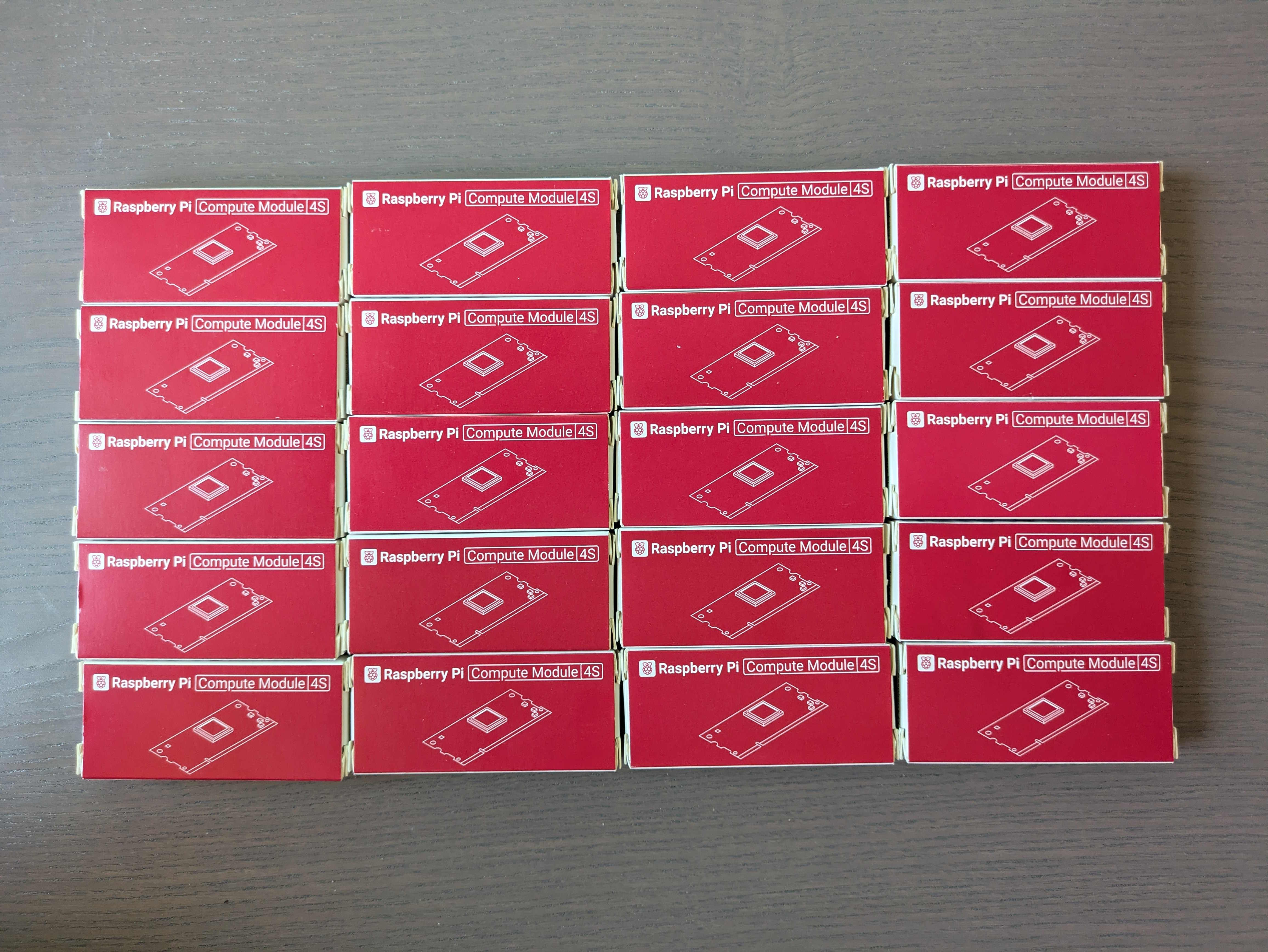
Unlike the normal Raspberry Pi Compute Module 4 (CM4), mine use the SODIMM socket and aren't compatible with the Compute Module 4 IO Board, which are needed to expose the interfaces of the board.
Given the CM3 IO boards are compatible with the modules I have, surely the best solution would be to get some of those, right? Almost: those would work, but because of the CM3's age, IO boards aren't being manufactured for those anymore, and on reseller markets they cost around $60 CAD. In comparison, IO boards for the normal CM4 like this Waveshare one are roughly half that.
Naturally, I didn't want to fork over a grand on IO boards. One of my first leads was an article and design by magkopian on Instructables: Design Your Own Raspberry Pi Compute Module PCB. I wanted to use this as the base for my own board design. Having never done circuits to this level, though, I needed to start somewhere easier.
Becoming Brighter
On the side, I was also making a clap activated LED strip based on a pretty simple circuit with a MOSFET and some resistors. I ended up getting one CM3 IO board from Waveshare just so I could at least see that the CM4Ss were functional, and I then used it to control the switch based on a microphone and a YAMNet classifier.
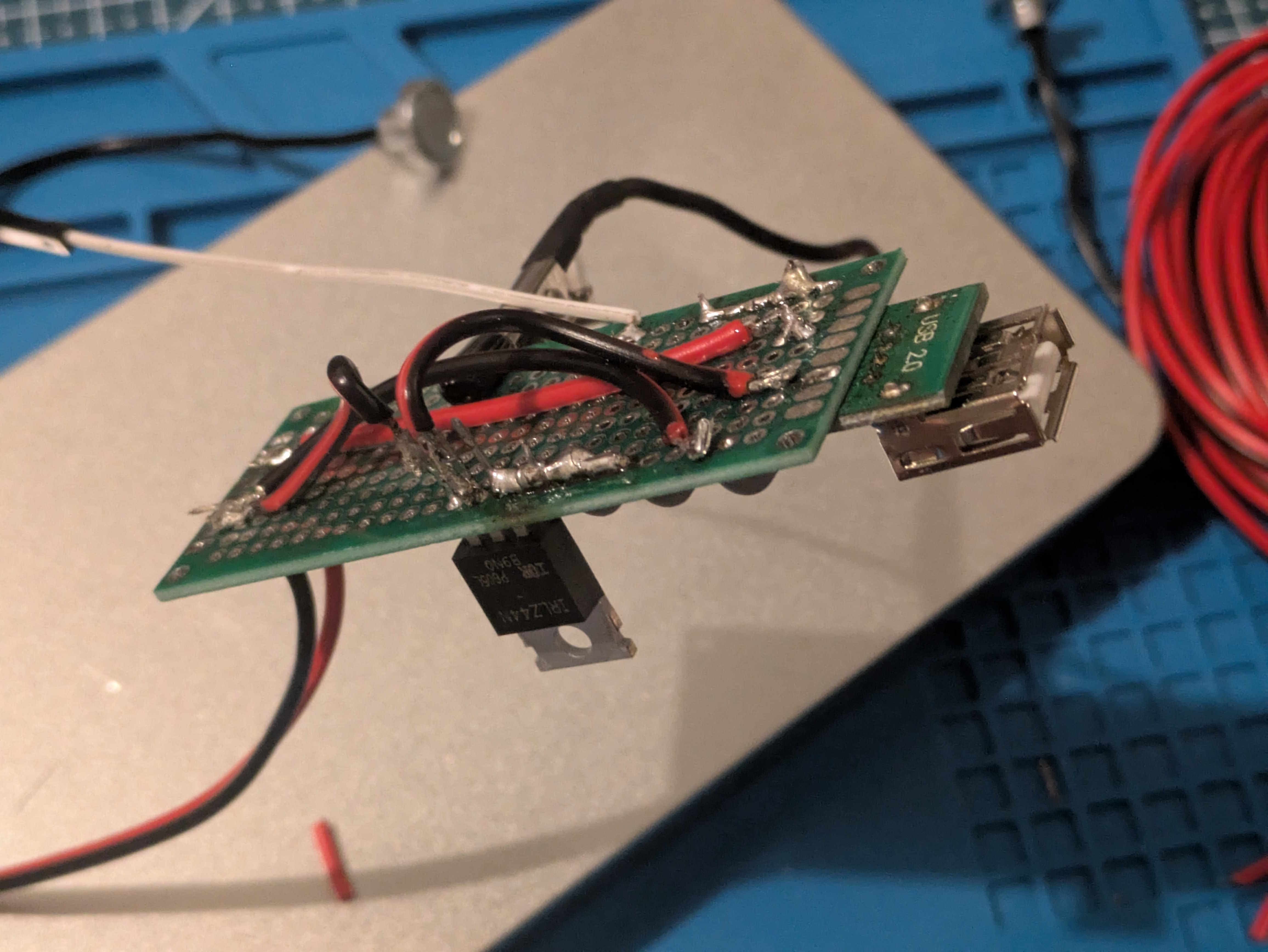
My first board was just an amalgamation on a protoboard.
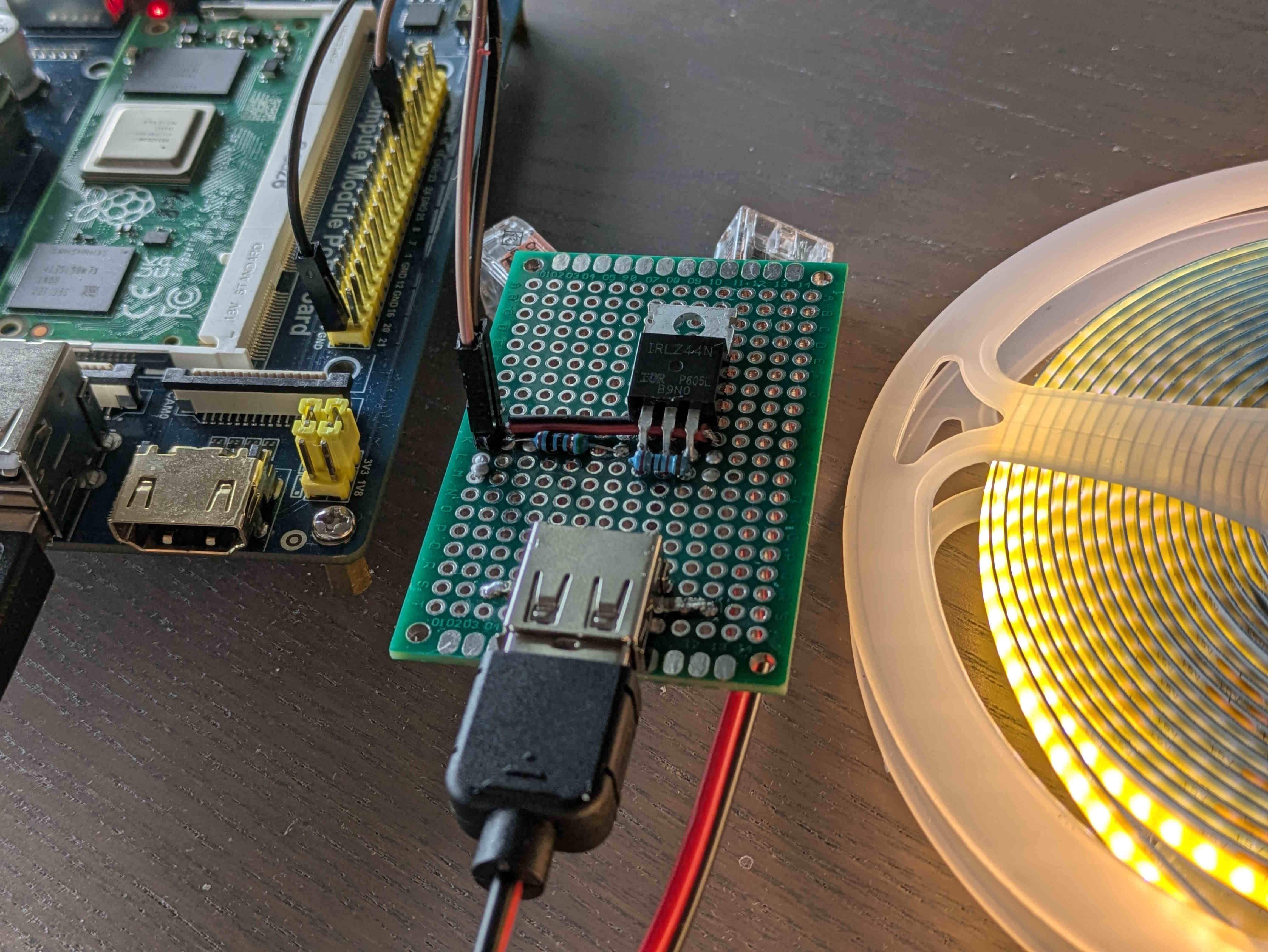
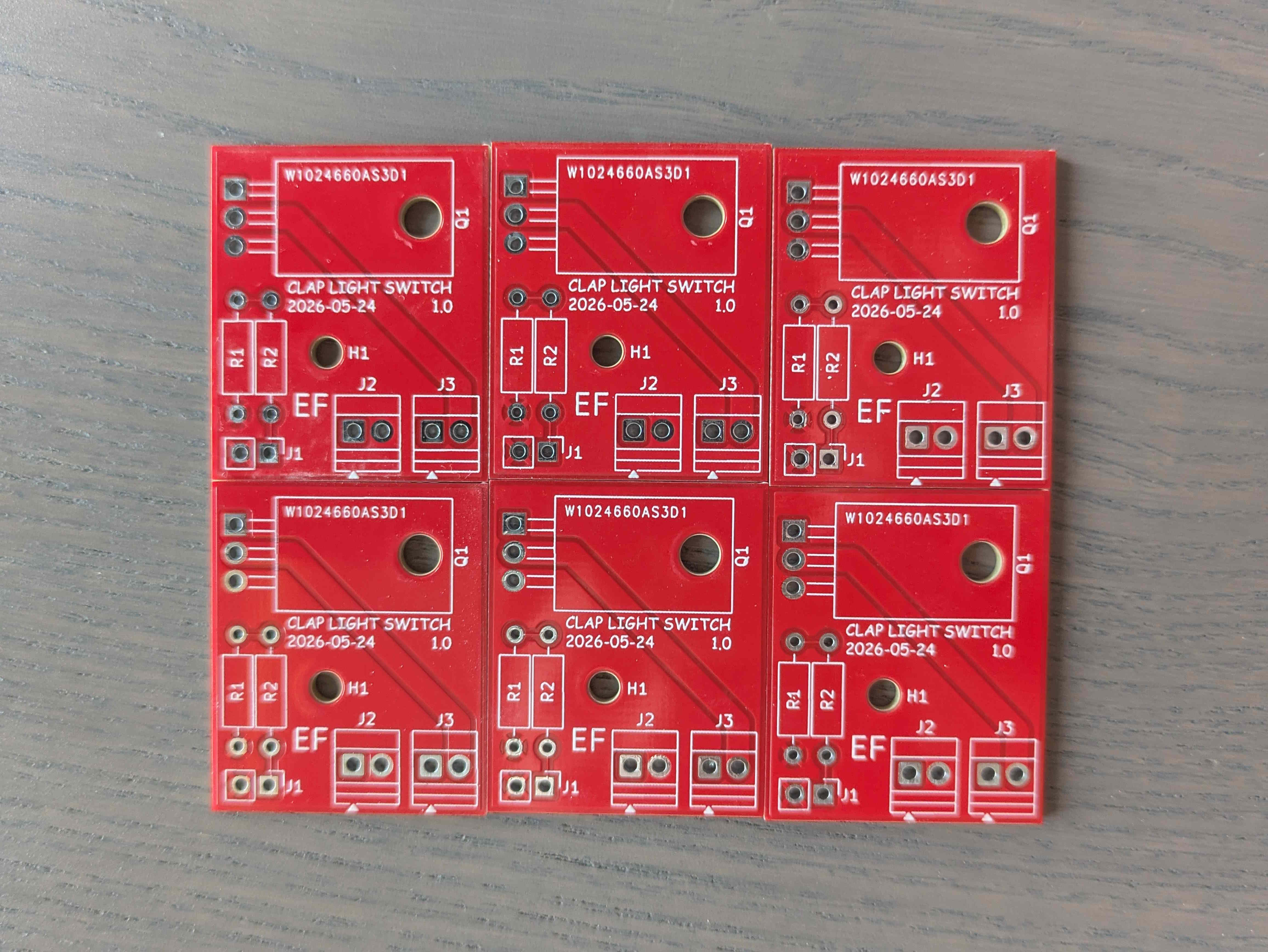
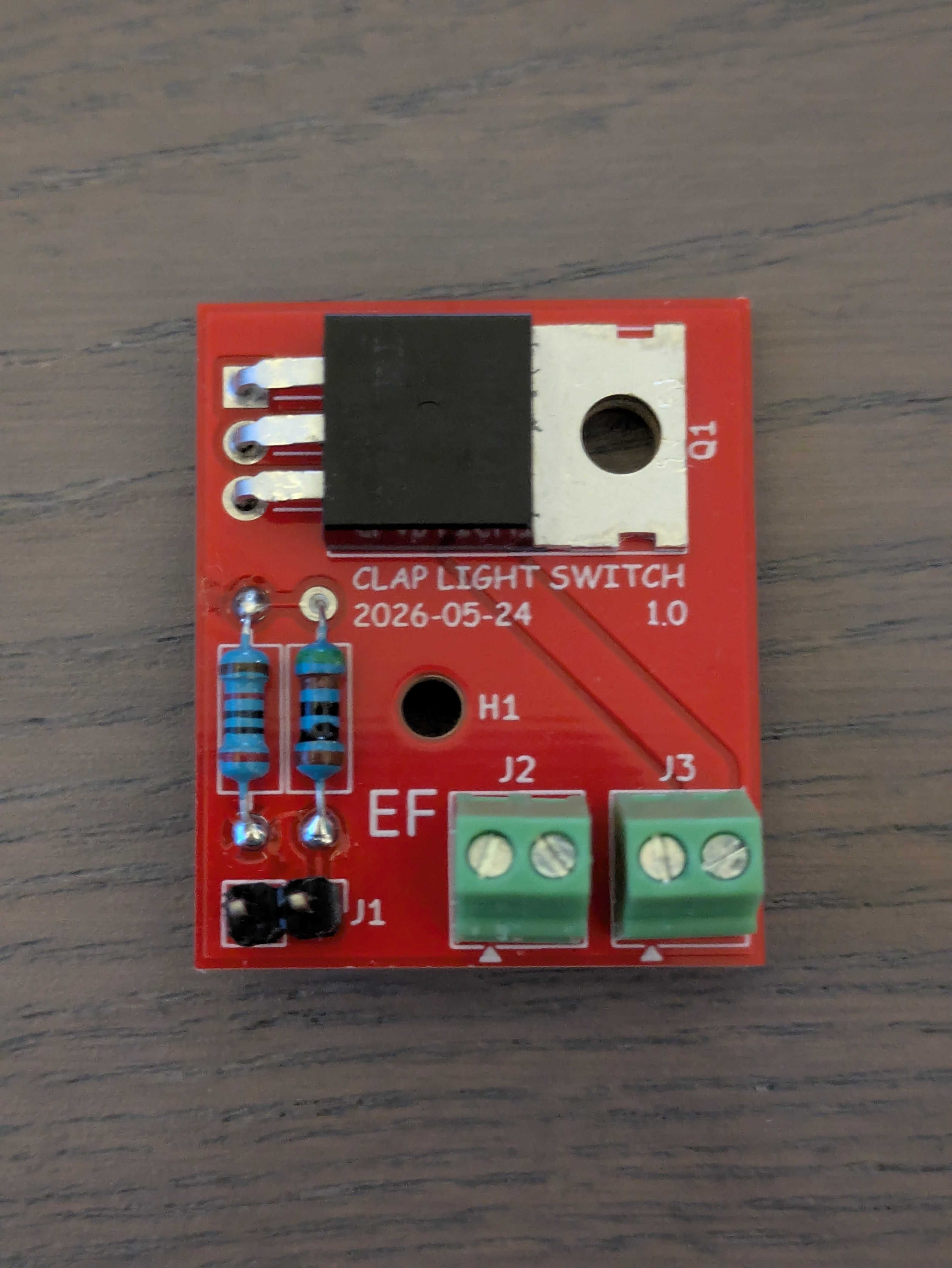
I refined it over 2 more revisions, before I decided to finally start making a PCB. I had never done that before, and it took a bit of time to finally get started. On a Saturday afternoon, I watched a bunch of KiCad tutorials and got started. About a day later, I had something that seemed decent. Because I already had parts on hand, I designed it for through-hole components.
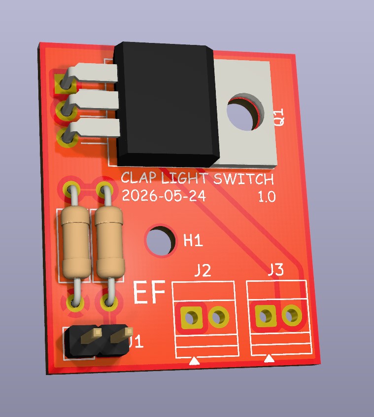
I decided to order it through PCBWay for not much reason other than they were a name I was familiar with (thanks to all those YouTube sponsorships presumably). All in, the boards cost me about $10 CAD and they arrived about a week after ordering.
90% Done, 90% Left
Having successfully designed a PCB and gotten it manufactured, I turned my attention back to the IO board. The aforementioned design by magkopian was made quite a while back with KiCad 6. My first goal was to migrate it over to KiCad 10 so I could modify it to fit my needs. Among other things, I wanted:
- the micro USB switched to USB C
- a slave USB C port to allow the flash onboard my CM4Ss to be programmed
- removal of the DAC since I didn't need it and it took up a lot of space
- more IO, as I wanted at least 2 USB A ports and an Ethernet port whereas it only had 1 USB A
Migrating the board to KiCad 10 took a bit as there were many footprint and symbol library changes plus a handful of weird schematic errors, presumably from the upgrade process. Migrating to USB C and adding a slave port didn't take too long though. The DAC removal was pretty easy.
The last major item was adding the extra USB A port and Ethernet. I pored over the schematics of the CM3 IO board I got (thank you Waveshare for having this available!) and noted they used the LAN9514 chip from Microchip. Using the same family of chip made sense as they were proven and had good Raspberry Pi support. I opted for the LAN9512 chip as that offered 2 downstream USB ports instead of the 4 of the 9514; I only wanted 2.
What I soon realized is how difficult this would be and how much uncertainty this would add to my design. With 64 pins on the chip, an external clock, and power filtering/regulation requirements, this was by far the most complicated part.
Over the next few months as I slowly worked on other TODOs on the IO board design, I mulled over how to approach this problem. I was losing confidence in this IO board actually working, and I wanted to see some results to help keep me excited about the project. In early September, I finally decided that I would need to design a board with the LAN9512 in order to get familiar with it and ensure my design actually functions.
Actually Designing the USB Hub
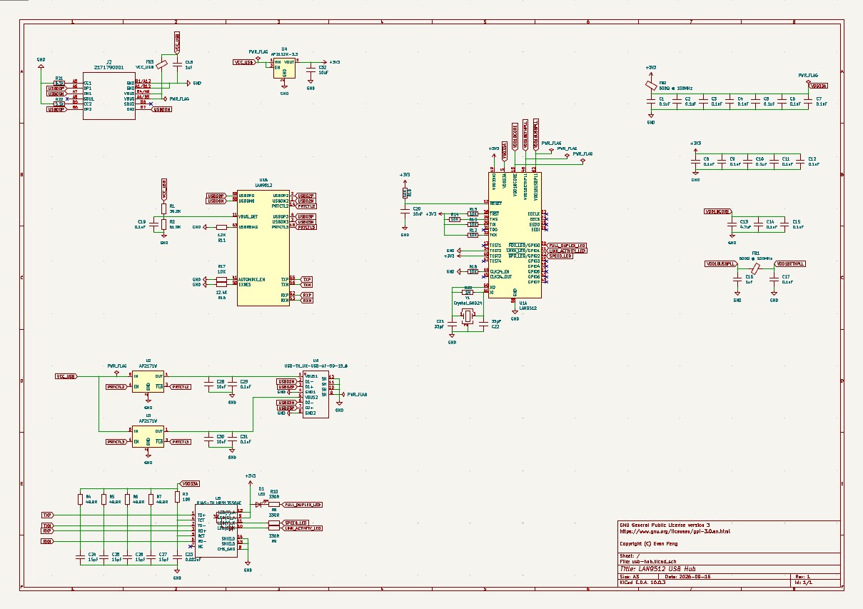
On September 9th, I sat down and began creating the schematic, which was largely based on the LAN9512 reference schematic. That gave me a lot to work with, but I still needed to figure out the input USB C port, 3.3V power regulation, specific component choices, which fab I wanted to use, and a whole lot of other smaller details.
The fab was one of the easier items. I wanted to try out JLCPCB, because their parts library seemed like it'd make life a lot easier. This is what I plan to eventually do for the IO board as well. There is a nice plugin for KiCad for JLCPCB which made selecting components and generating all the Gerber/production files super easy. I would highly recommend this setup. (note: it's not perfect and did crash a few times when trying to export files. Wasn't a huge deal though)
Back when I added USB C to the IO board, I found a nice Molex USB C part that fit nicely here. Although there were many other cheaper options, I decided to use the Molex 2171790001 because it offered USB 2.0, supported up to 5A, had a nice footprint and a 3D model, and was single-row. This didn't take too long to add to the schematic.
USB port power control took a while of staring at the datasheet and reference implementation to figure out. Naturally, Microchip's reference implementation uses another one of their chips for this, the MIC2026-1BM. I had originally thought to use 2 poly fuses + diodes, as shown in Figure 2-4 (page 15), but considering that an IC would be able to more accurately limit power and use the PRTCTL pins, I chose the AP2151WG-7 from Diodes Incorporated instead. The IC solution also meant one less unique (extended) component, which mattered later when I looked at assembly costs.
For power regulation, I only need 3.3V as the LAN9512 has an onboard regulator for whatever it needs 1.8V for. Based on the typical power consumption, I originally picked the AMS1117-3.3 as it comfortably fit the LAN9512's power consumption numbers. Later though, I discovered that its datasheet strongly recommended a tantalum capacitor for stability reasons. Later on, to reduce the use of extended parts, I switched to the AP2112-3.3V, which stated ceramic ones were fine. This had a lower current rating at 600mA vs 1A, but this was still comfortably above the LAN9512's ~250mA maximum typical draw.
An important aspect I learned about Ethernet ports is their magnetics. I had wondered why some parts were much cheaper than others. These didn't seem like particularly well-known brands either, so it wasn't name recognition. By also cross-referencing the schematics, I learned some Ethernet ports have magnetics for noise reduction and stuff like that. I am by no means well versed in this stuff, but this was enough to determine that I should find an Ethernet part that includes them.
Getting the symbols and footprints was a bit of a pain for the USB and Ethernet ports. JLCPCB has both available for EasyEDA users, but given that I was using KiCad, that seemed like a non-starter. It turns out there is a website that can export those to a KiCad format, which was super helpful. Be warned, though: the symbols/footprints may have issues. At the last minute before ordering, I found an issue where the Ethernet footprint was missing holes for its plastic through-hole nubs.
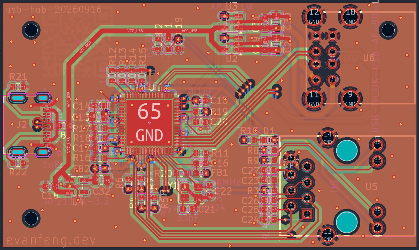
With the schematic mostly complete (I'm not writing things fully in chronological order for ease and clarity!), I started the routing and layout with board configuration. I needed 4 layers to achieve the correct impedance for USB/Ethernet, so that was a quick choice. Importing a JLCPCB capabilities template would ensure I designed boards that were possible to make and wouldn't incur extra charges. I also set the default trace parameters by netclass: I used JLCPCB's impedance calculator to find the right spacing and width for the differential traces, along with KiCad's trace width calculator and estimated power ratings.
Routing was a bit painful, and I spent way longer on it than I probably should have. I wanted it to be fairly visually appealing, so I worked on the USB and Ethernet traces first. It was hard to tell how big the board needed to be and where components should go. I ended up swapping the Ethernet and USB port locations and moving around the ~65 components I had. The LAN9512 Hardware Design Checklist was super useful for figuring out which resistors or capacitors should be near what. By the end, I had a 40mm x 67mm (😏) board with signal layers on layers 1 and 4, a ground plane on layer 2, and some power routing on layer 3.
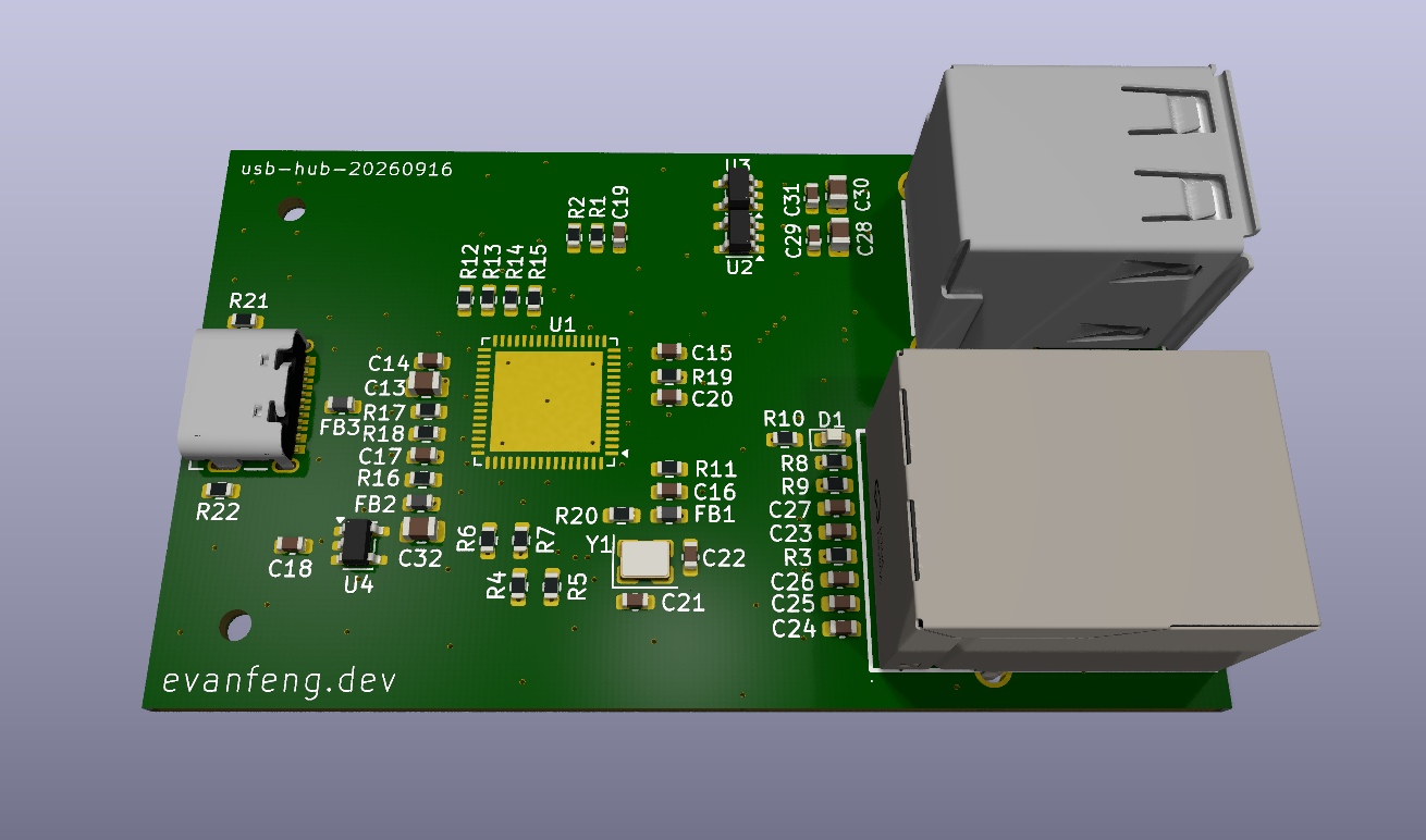
With helpful input and reviews from Maximus and Riggy, I was ready to order the board. Or so I thought, until I looked at the JLCPCB price quote: nearly $300 for 5 assembled boards. That was way too much, but thankfully a lot of it was reducible.
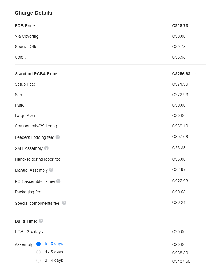
JLCPCB classifies parts from their libraries into 2 main categories: basic and extended. For each unique extended part type in the design, they charged $4 to switch the reel on their pick-and-place machine. I had around 15 of these, which made that fee add up to almost the same as the parts themselves ($57 vs $69). To fix this, I was able to change most of my parts over to basic ones, though some were unavoidable like the LAN9512, clock crystal, and a handful of other components.
The other large driver of cost was opting for standard PCB Assembly (PCBA). JLCPCB has an 'economic' type which is way cheaper, but this limited me to only assembling one side of the board and perhaps more devastatingly, I could only have green PCBs whereas I wanted purple. To make the most out of the one-sided assembly, I moved as many components to the front as I could, leaving 12 capacitors on the back for power filtering. I made the footprints of these 12 larger so that they'd hopefully be easier to solder on myself.
Finally, the last way to reduce cost was just to have fewer boards assembled: 2 instead of 5.
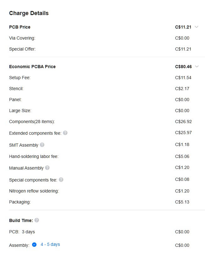
With all these cost reductions, I got the cost down to about $100 CAD. JLCPCB was also offering a discount if I placed the order using their new desktop app, so I obliged. It's probably spyware or something but even after some surprise shipping and import fees, the total came out to $104 CAD thanks to it.
While I waited for the boards to be manufactured and assembled, I obtained the capacitors I needed for the backside of the board along with some solder paste.
I got Board
The boards arrived about 2 weeks after I ordered them, and I think they look pretty good. It's awesome to see custom engineered fiberglass holding circuits that I designed, printed with my own silkscreening.
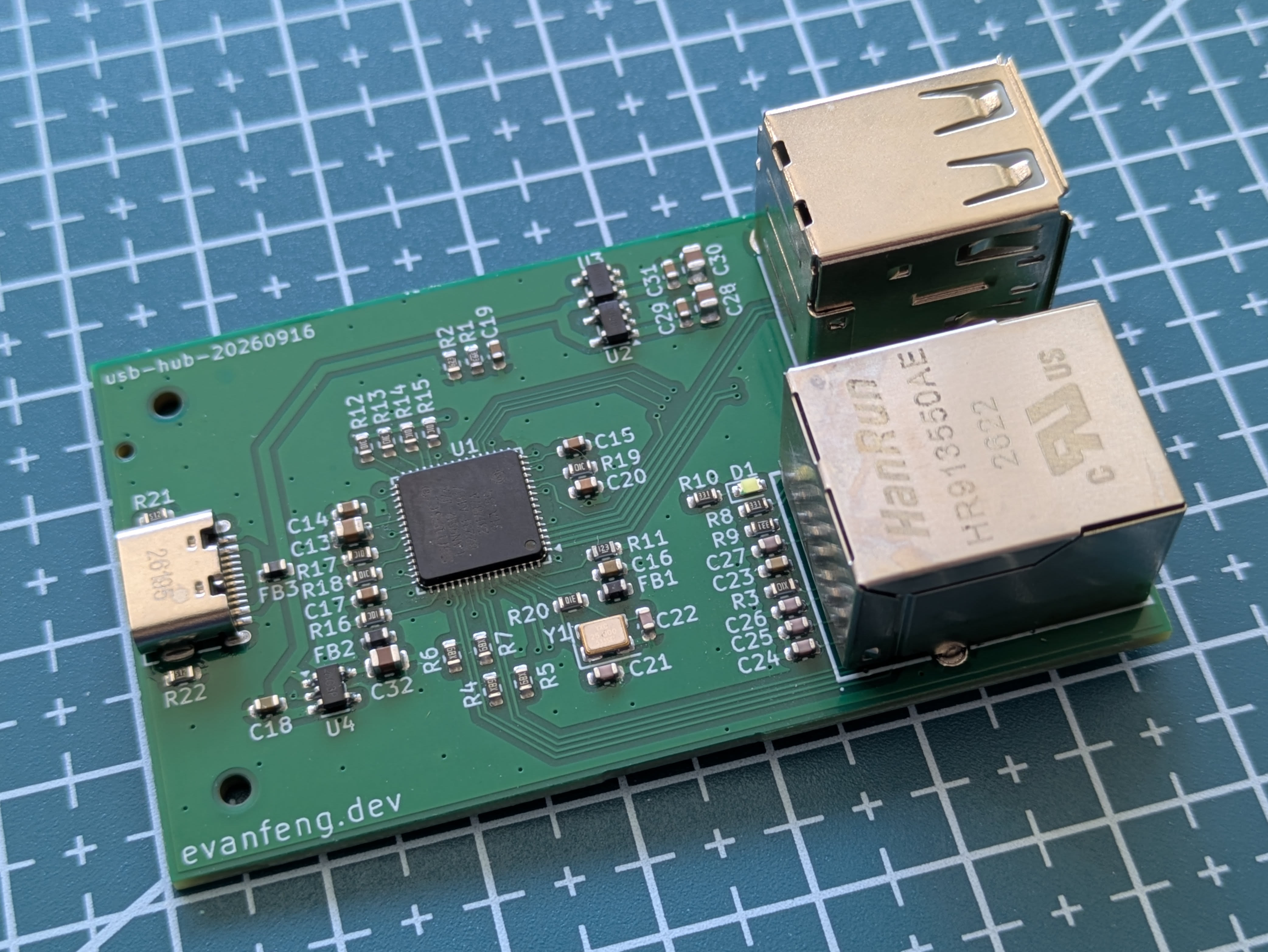
Although I had all the parts and supplies to get the 12 capacitors soldered on the back, I lacked the equipment. Lacking patience to get access to a rework station, I deemed it safe enough to just see what happens when some filtering capacitors are missing.
I did some basic checks to ensure the power rails weren't shorted, and then plugged it into a USB wall outlet to see if it would go up in a puff of magic smoke. It didn't: with confidence, I then plugged it into my Raspberry Pi's USB port.
[1480437.610180] usb 1-1.2: new high-speed USB device number 5 using dwc2
[1480437.698632] usb 1-1.2: New USB device found, idVendor=0424, idProduct=9512, bcdDevice= 2.00
[1480437.698670] usb 1-1.2: New USB device strings: Mfr=0, Product=0, SerialNumber=0
[1480437.699494] hub 1-1.2:1.0: USB hub found
[1480437.700303] hub 1-1.2:1.0: 3 ports detected
[1480437.978161] usb 1-1.2.1: new high-speed USB device number 6 using dwc2
[1480438.066500] usb 1-1.2.1: New USB device found, idVendor=0424, idProduct=ec00, bcdDevice= 2.00
[1480438.066533] usb 1-1.2.1: New USB device strings: Mfr=0, Product=0, SerialNumber=0
[1480438.069659] smsc95xx v2.0.0
[1480438.182868] SMSC LAN8700 usb-001:006:01: attached PHY driver (mii_bus:phy_addr=usb-001:006:01, irq=47)
[1480438.184816] smsc95xx 1-1.2.1:1.0 eth1: register 'smsc95xx' at usb-fe980000.usb-1.2.1, smsc95xx USB 2.0 Ethernet, b8:27:eb:73:48:d6
[1480438.270415] smsc95xx 1-1.2.1:1.0 eth1: hardware isn't capable of remote wakeup
[1480438.278369] smsc95xx 1-1.2.1:1.0 eth1: Link is Down
dmesg showed everything coming up fine, surprisingly. It was beautiful. Ethernet came up too, once I plugged it in:
[1481153.693144] smsc95xx 1-1.2.1:1.0 eth1: Link is Up - 100Mbps/Full - flow
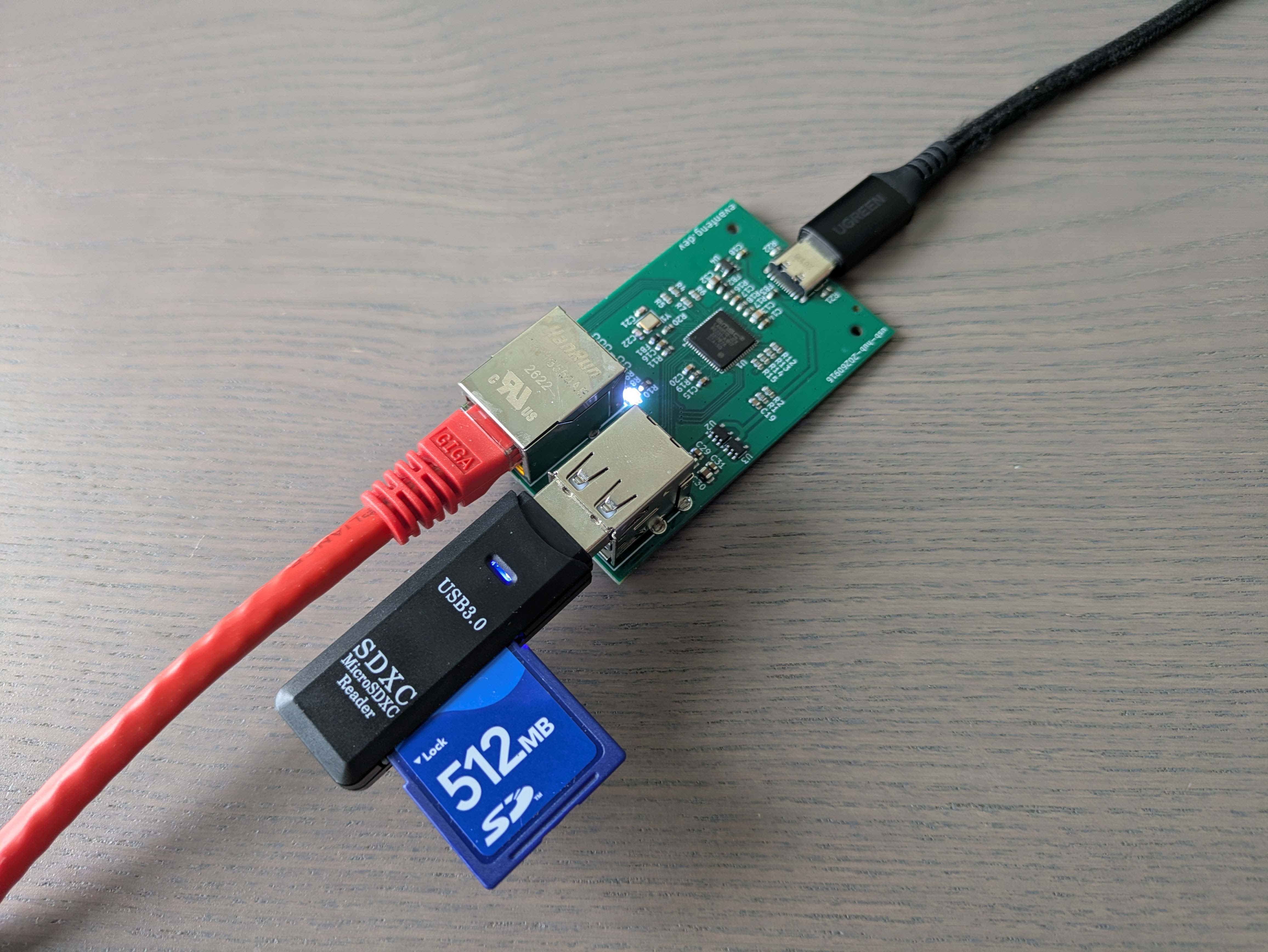
Having gone beyond my expectations, I decided to try it out on my Windows machine. I half expected it to fail, perhaps because of missing drivers or because Windows might not supply it a unique MAC address. But, it did! I tested the USB ports, and they worked as you'd expect. I didn't see any flakiness either, even though those 12 capacitors for the two 3.3V rails were just flat out missing.
What's Next
Now, I'm fairly confident I can integrate extra USB and an Ethernet port onto my IO board design. Once I find the time to resume development and finish the IO board, I'll consider doing another write-up like this one.
There are a handful of things I'd change when I do integrate it:
- use smaller components, as it turns out 0603 is still quite big and leaves room in the specifications (ie voltage for capacitors)
- this would also likely allow me to avoid capacitors on the backside of the board
- round the corners of the board
- have the correct date silkscreened onto the board
- make the board denser, since I want the Pi IO board to be small-ish
- consider exposing test pads for the main power rails (ie VCC_USB, VDD33A, etc)
- find other fun things to silkscreen onto the board
For the USB hub specifically, it has probably taken around 50 hours of work from staring at the LAN9514 schematic to connecting to the internet with it: time well spent, I feel.
Thanks again to Maximus and Riggy for their help with this project :)
The KiCad design files can be found at https://github.com/evenevan/usb-hub.